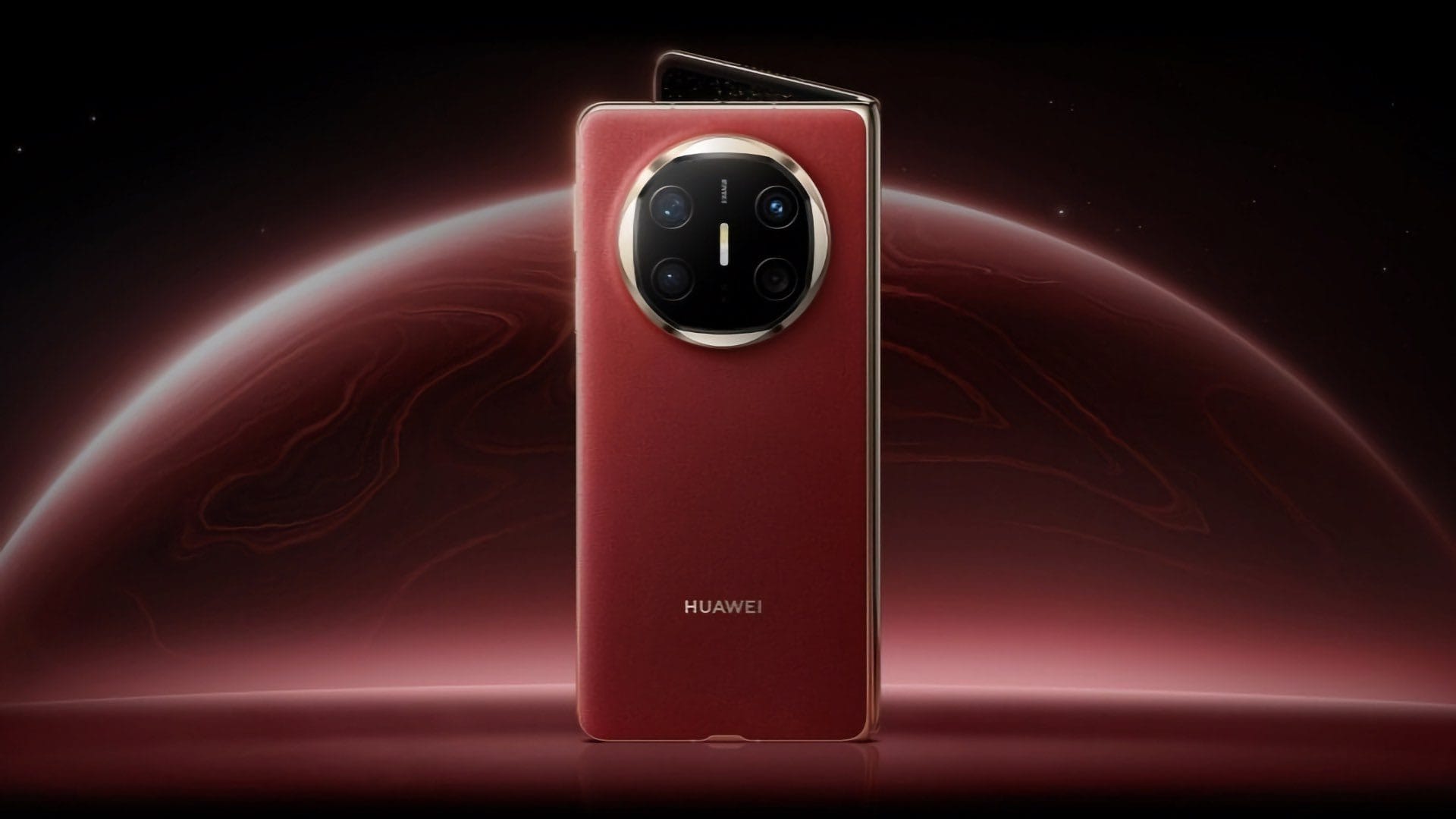
Huawei has unveiled its Tau Scaling Law, targeting 1.4nm-equivalent chip performance by 2031 through a LogicFolding 3D-stacking technique designed to bypass US export-controlled lithography equipment. As reported by Nikkei Asia, the Chinese tech giant announced this roadmap at an international scientific conference, marking its most ambitious attempt yet to overcome American semiconductor restrictions.
Key Takeaways
- Huawei announced its Tau Scaling Law roadmap targeting 1.4nm-equivalent chip performance by 2031.
- The LogicFolding 3D-stacking technique aims to bypass US export-controlled EUV lithography machines.
- Semiconductor analyst Ian Cutress calls the goal ‘very ambitious’ and questions its feasibility.
- Success could reduce China’s reliance on Western chipmaking technology and reshape global supply chains.
What is Huawei’s Tau Scaling Law?
Huawei’s Tau Scaling Law represents a fundamental shift away from traditional Moore’s Law scaling, which relies on shrinking transistor sizes using advanced lithography. According to Huawei’s announcement, this new approach centres on LogicFolding, a 3D-stacking technique that packs more transistors into smaller spaces without requiring extreme ultraviolet (EUV) lithography machines.
The technique essentially stacks multiple layers of logic circuits vertically, achieving performance improvements through density rather than traditional node shrinking. Huawei claims this method can deliver 1.4nm-equivalent performance by 2031 — a timeline that would put it ahead of many Western competitors who rely on ASML’s EUV machines, which are banned from export to China under US sanctions.
One reason this matters is that current Huawei smartphones in the UAE market use older chip architectures due to these restrictions. If successful, the Tau Scaling Law could enable significantly more powerful processors in future Huawei devices.
How does LogicFolding work in practice?
LogicFolding builds transistor circuits in three dimensions rather than the traditional flat, two-dimensional approach. According to industry analysis, this involves stacking multiple silicon layers and connecting them through vertical interconnects, similar to building a skyscraper instead of expanding horizontally.
The technique addresses the physics problem that has plagued Moore’s Law — as transistors shrink below 3nm, quantum effects make them increasingly difficult to control. By stacking layers instead, Huawei aims to achieve equivalent density and performance without pushing into these problematic size ranges.
However, 3D stacking introduces its own challenges. Heat dissipation becomes exponentially more difficult with multiple active layers, and manufacturing defects in any layer can compromise the entire chip. These are the engineering realities that make experts sceptical of Huawei’s 2031 timeline.
Why experts doubt the 2031 timeline
Semiconductor analyst Ian Cutress called Huawei’s claims ambitious to the point of questionable. In commentary on X, Cutress said the announcement “doesn’t look like a huge breakthrough” and described it as a technique “expected to be done by everyone” because Huawei “can’t scale litho” and is accelerating other parts of the roadmap.
The scepticism stems from practical engineering limits. Current 3D stacking technology, used in products like Samsung’s memory chips, typically handles two to four layers. Achieving 1.4nm-equivalent performance would likely require significantly more layers, creating thermal management problems that no company has solved at scale.
Cutress added that even if Huawei ships chips using this approach in 2026 or 2027, the company “still has a way to go to hit 14A equivalents by 2031 using SMIC multipatterning.” The gap between announcement and engineering reality often proves wider than companies initially estimate.
What this means for the global chip industry
If Huawei succeeds, the implications extend far beyond technical achievement. China would effectively leapfrog Western semiconductor restrictions, potentially reshaping global supply chains and reducing dependence on US-controlled technologies. This connects to broader tensions around chip export controls and technological sovereignty.
For consumers in markets like the UAE, success would mean newer Huawei devices in the region would no longer be capped by current chip restrictions. Current Huawei phones in the region use older architectures due to sanctions, limiting their performance capabilities.
The announcement also signals China’s long-term strategy to build parallel technology infrastructure. Rather than trying to catch up with existing Western approaches, companies like Huawei are exploring alternative paths that could eventually prove superior. This parallels developments in AI technology where Chinese firms pursue different architectures.
Frequently Asked Questions
What is Huawei's Tau Scaling Law?
Huawei’s Tau Scaling Law is a new roadmap aiming to achieve 1.4nm-equivalent chip performance by 2031 through LogicFolding 3D-stacking technology, bypassing the need for US export-controlled EUV lithography machines.
How does Huawei's LogicFolding technique work?
LogicFolding stacks multiple layers of transistor circuits vertically rather than shrinking them horizontally. This 3D approach aims to increase chip density and performance without requiring advanced lithography equipment banned under US sanctions.
Can Huawei really make 1.4nm-equivalent chips without EUV?
Semiconductor experts express significant doubt. Ian Cutress from TechInsights calls it ‘very ambitious’ and notes the industry already struggles with advanced packaging complexities, making Huawei’s timeline questionable.
What are the implications of Huawei's new chip technology for the semiconductor industry?
Success would reduce China’s reliance on Western technology, potentially reshape global supply chains, and intensify technological competition. It could also lead to more powerful Chinese devices in markets like the UAE.